Chip
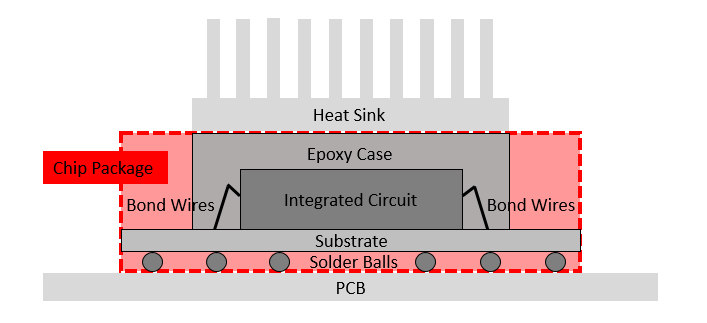
Chips are modules made of semiconductor material on which integrated circuits are embedded. Chips generate excess heat and thus require cooling to improve reliability and avoid premature failure.
The following image displays the various elements of a chip package:
To represent the geometry of a chip package, the
Electronics Cooling Toolset supports the following
 Chip QuickParts:
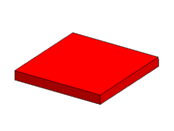
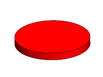
If the built-in shape templates are not suitable, you can define a
 Custom chip whose geometry is based on a
Construction Geometry that you specify.
Custom chip whose geometry is based on a
Construction Geometry that you specify.
To represent the physics of a chip package, two thermal modeling approaches are available:
- Solid model: represents the chip package as a single solid part of a specified material. A total heat source models the excess heat of the package.
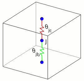
- Compact thermal model (CTM) ([144], [145]): a simplified component model that mimics the performance of the chip package within the system-level analysis. It represents the critical heat flow paths within the package using a thermal resistor network. Each network node corresponds to a surface of the package or a region within the package and is associated with a single temperature.
A CTM of a chip package is more accurate than a solid model. As a CTM does not require a volume mesh within the package, it is also computationally less expensive. On the other hand, the resistor network of a CTM requires that you have access to detailed information about the heat flow paths within the package. The following types of resistor networks are available:
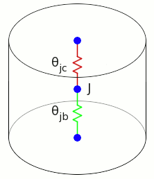
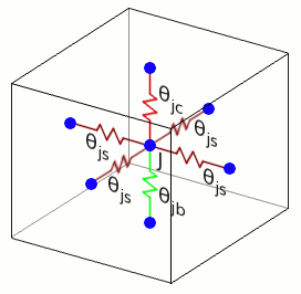
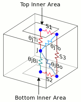
- Junction node—that represents the integrated circuit.
- Case node—that describes the top surface of the package.
- Board node—that is considered as the contact between the package and the PCB.
Two resistor and Delphi networks are suitable for packages where the heat transfer through the sides can be ignored. For example, within a typical BGA (ball grid array) package most of the heat flows through the solderballs to the PCB at the bottom and/or to the heatsink on top. A two resistor network assumes uniform temperatures on the top and bottom surfaces, whereas a Delphi network relaxes this assumption by allowing different temperature in the inner and outer areas of the surfaces.
Star networks are suitable for packages where the heat transfer through the sides can not be neglected. For example, within a leaded package the heat flow path through the sides significantly affects the package temperature. The available star network assumes a uniform temperature across the side surfaces.
Within the Electronics Cooling Module, each network node—apart from the junction node—corresponds to a QuickPart Surface of constant and uniform temperature. Surfaces without a network node are modeled as adiabatic. For more information, see Resistor Networks Formulation.
Chip—Properties
The following properties are common to all types of chip packages:
| Name | Specifies the name of the chip under which it is stored in the tree. | |
| Geometry |
|
|
| Placement | See Placement properties. | |
| Physics |
|
|
The following properties characterize the different geometrical types:
Block—Specific Properties
| Geometry |
|
|
Cylinder—Specific Properties
| Geometry |
|
|
Custom—Specific Properties
| Geometry |
|
|
The following tables display the properties of the available resistor networks:
| Note | Request the required input values from the package supplier or derive them from JEDEC-standard thermal tests. Alternatively, you can extract the values from a detailed thermal model of the package using a statistical optimization process that minimizes errors in junction and surface temperatures for a variety of environmental conditions. |
Two Resistor
 |
 |
||
|
|||
Star Network
 |
||
|
Delphi Network
 |
||
|