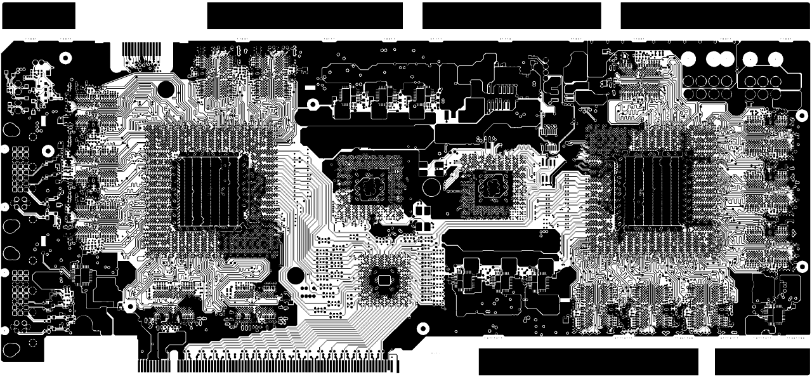
PCB

Printed circuit boards (PCBs) route signals and power between electronic components. They typically assemble conductive tracks and dielectric laminates in multiple layers.

The Electronics Cooling Toolset supports the following geometry templates for PCB QuickParts:

  • Rectangular
  • Circular

If the built-in geometry templates are not suitable, you can define a Custom PCB whose geometry is based on a Construction Geometry that you specify. The specified geometry must be a straight extrusion from a planar face. Tapered extrusions are not supported.

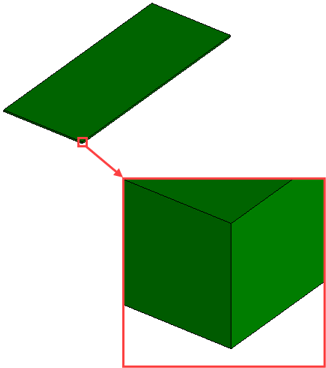
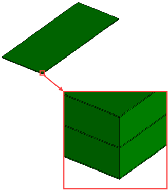
To represent the physics of a PCB, the following modeling approaches are available:

Basic
The basic approach represents the PCB as a single solid part.
To specify the thermal conductivity of the PCB, the following options are available:
  • Specify material—sets a single PCB material. The thermal conductivity is constant throughout the PCB.
  • Specify layers—sets multiple layers of metal and dielectric material. The thermal conductivity of the PCB is modeled as anisotropic. It is calculated as a function of the layer count, each layer's thickness and metal fraction, and the thermal conductivities of the metal and dielectric material. See Eqn. (563).
Detailed
The detailed approach represents the PCB as a composite of multiple layered solid parts.
To model the thermal conductivity of each layer, the following options are available:
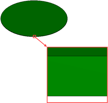
  • Specify metal fraction—sets the fraction of metal in the layer. The thermal conductivity is isotropic throughout the layer and calculated as a function of the metal fraction and the thermal conductivities of the metal and dielectric material. See Eqn. (567).
  • Specify image file—imports a bitmapped image that represent the layer's metal content.

    Example:


    Based on the image grayscale (0 - 255, where 0 = all dielectric and 255 = all metal), the Electronics Cooling Toolset localizes the metal and creates a thermal conductivity map. See Eqn. (568). This map is then converted into a table and mapped onto the volume mesh of the respective layer.

If you have IDF files that contain board and its components' layout definitions, you can import the files (see Import IFD file action). The Electronics Cooling Toolset automatically creates a PCB QuickPart for the board and Generic QuickParts for the components.

PCB—Properties

The following properties are common to all types of PCBs:

Name Specifies the name of the PCB under which it is stored in the tree.
Geometry
Local Origin
Specifies the position of the PCB's local coordinate system. See X_or, Y_or, Z_or in the Graphics window. It is used for placing the PCB in the simulation domain. The following options are available:
  • Bottom Center: Center of the Zmin face.
  • Bottom Center of Range Box (IDF import only): Center of the bottom face of the bounding box.
  • Bottom Corner 1 (rectangular PCB only): Xmin/Ymin/Zmin corner of the rectangle.
  • Bottom Corner 2 (rectangular PCB only): Xmin/Ymax/Zmin corner of the rectangle.
  • Center: Center of the geometry.
  • Center of Range Box (IDF import only): Center of the box that bounds the imported geometry.
  • Custom: This value appears when you set the local origin interactively within the Graphics window, see Placing Object Interactively.
  • IDF Default Reference (IDF import only): As specified in the IDF file.
Placement See Placement properties.
Physics
Heat Source
Specifies the total heat generated by the PCB.
Rectangular/

Circular/

Custom

Thermal Specification
Controls if the thermal conductivity of the PCB is modeled as material dependent or as layer dependent. The following options are available:
  • Specify Material: Allows you to set a uniform Material throughout the PCB. You can choose the material from the Solid Sim Materials that you define in the Setup panel.

    If the Thermal Conductivity property of the respective material uses the Anisotropic method, you set the components of the Thermal Conductivity tensor using the principal tensor method. See Principal Tensor. The XX Component, YY Component, and ZZ Component are defined with respect to the axis of the QuickPart's local coordinate system. See X_or, Y_or, Z_or in the Graphics window.

  • Specify By Layer: Allows you to set the Number of Layers, the Metal Material—that is the material of the conductive tracks and layers—, and the Dielectric Material—that is the laminate material. A table editor enables you to specify the Name, Thickness, and Metal Fraction for each layer. For a Custom PCB, you need to set a PCB Normal to control the orientation of the layers.
Rectangular Detailed/

Circular Detailed/

Custom Detailed

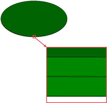
You set the Number of Metal Layers, the Metal Material (material of the conductive tracks and layers), and the Dielectric Material (the laminate material). A table editor enables you to specify a Name, Thickness, and Mode for each metal layer and each intermediate dielectric layer. The PCB Thickness (read only) displays the overall thickness of the PCB.

The Mode of a layer controls how the thermal properties of the layer are modeled. The following options are available:

  • Metal Fraction—allows you to specify the fraction of metal in the layer. The thermal conductivity is fraction-averaged across the layer.
  • Image File—allows you to import an image file (*.png, *.jpg, *.tiff, *.pnm, or *.bmp ) of the layer's metal content.

    In the Graphics window, the image is displayed next to the top layer of the PCB (regardless of the layer for which it is imported).

    The following properties allow you to adjust the imported image according to your needs:

    • [layer] - Image Rotation—allows you to rotate and flip the image.
    • Resolution Scale Factor—allows you to reduce the pixel count of the image. Reducing the pixel count reduces the computational cost to calculate the thermal conductivity map and to convert the map into a table. Note that reducing the pixel count also reduces the accuracy of the table.

The following geometry properties characterize the different types of PCBs:

Rectangular—Specific Properties

Geometry
X, Y
Specify the dimensions in x- and y-direction, in the PCB's local coordinate system. See X_or, Y_or, Z_or in the Graphics window.
Thickness (not for Detailed PCB)
Specifies the extent of the rectangular PCB from bottom to top.

Circular—Specific Properties

Geometry
Radius
Specifies the radius of the circular outline.
Thickness (not for Detailed PCB)
Specifies the length that the circular PCB extends from bottom to top.

Custom—Specific Properties

Geometry
Selected Construction Geometry
Specifies the Construction Geometry that describes the geometry of the PCB. If you select multiple Construction Geometries when creating a Custom PCB, the Electronics Cooling Toolset automatically creates multiple PCBs that own the same physics properties.

IDF Import—Specific Properties

Geometry
Height
Specifies the thickness of the imported PCB.